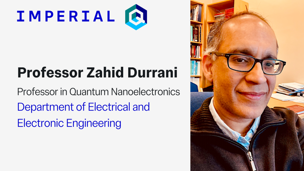
Professor Durrani is a Professor of Quantum Nanoelectronics in the Department of Electrical and Electronic Engineering at Imperial College London. In this blog post, he shares more about his research as part of QuEST (Centre for Quantum Engineering, Science and Technology at Imperial College London). Professor Durrani works in the field of quantum nanoelectronics, investigating a means to process and store information in new, more efficient ways.
Can you tell us about your research area?
I work in the field of quantum nanoelectronics. This area concerns the development of nano and atomic scale semiconductor devices which directly exploit quantum effects, for applications in highly scaled, ultra-low power integrated circuits, and in quantum computation. Effects such as single electron charging and tunnelling, the formation of quantum wells and their energy states, and electron wavefunction control, can provide a means to process and store information in new, more efficient ways.
What led you to study this area?
I started out as an electrical engineer. The subject I loved the most in my undergraduate degree was semiconductor devices, which then led me to a master’s degree in Microelectronics and Semiconductor Physics, and then a PhD in Physics, investigating arrays of resonant tunnelling nanodevices. I have stayed in the quantum nanoelectronics area ever since, in both Electrical Engineering and Physics departments in universities, and often in collaboration with the semiconductor industry, e.g. Hitachi and IBM. I ‘balance’ on the fence between Physics and Engineering – I like to think this gives me a nice vantage point (or is it superposition?) on both!
What are the main aims of your current research?
In recent years, I have been working on the development of single atom, single-electron, quantum dot transistors and memory devices in silicon, capable of room-temperature operation. Here, information is defined using one electron per bit, and may be manipulated by controlling the electron as a particle, or at the wave function level. The development of these devices may enable great reduction in the energy consumption of large-scale integrated circuits, and allow Moore’s Law scaling of device size to continue to single nanometre, or even atomic scales. These devices, and the single electron control they provide, are also of great interest in studying the thermodynamics of energy and entropy in the single particle ‘Landauer’ limit, and for experimental investigations of Szilard’s single particle heat engine.
How could this research potentially benefit society?
One of the major challenges in electronics concerns the reduction of energy consumption in computation systems. Currently, with the rise of machine learning and large data processing applications, the energy demand for computation is increasing exponentially. We seem to be moving towards ‘strapping a power station’ to a data centre – clearly, this is unsustainable and to my mind, quite concerning. Reducing the power consumption of integrated circuits is crucial, and my research directly addresses this.
What are the next steps in your research? Are there any challenges ahead?
While I am always amazed by how far the semiconductor industry has pushed classical device minimum feature sizes, currently at the sub-10 nm level, there are great challenges at the 1 nm and smaller scale, as the device becomes fully quantum is operation. Control of device structure at this level is essential to properly manipulate and exploit quantum effects. Currently, nanofabrication methods lack the precision to fabricate large numbers of atomic scale devices with similar electrical characteristics, essential for practical quantum integrated circuits. This is the major, though I think surmountable, challenge!