Materials Science in the real-world: Insights from our student placement
Divija Sachdeva and Roman Ogorodnov, two undergraduate students from the Department of Materials, have recently finished their learning placement at AlixLabs in Sweden. Throughout their placement, they conducted an investigation into semiconductors fabrication.
Divija and Roman sought out their placements through networking and direct applications on LinkedIn. Their placements were independently funded and conducted during the Easter break.
In this blog post, they share more about their placement, what they learned and how this will positively impact their future studies.
Being Materials Science students, every day, we learn more about the pillars of its foundation and the technologies in the current modern world that are still in the developing phase. We start this degree with a rough (engineering) drawing of what our future aspirations are, which soon become the drive to be a part of the revolution for new sustainable and revolutionary materials. Roman and I wanted to learn more about the fabrication of semiconductors and advanced transistors because of our heavy interest in exploring how the new techniques for etching are being developed and being a part of it.
Our placement with AlixLabs
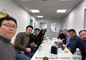
In April 2023, we had the opportunity to interact with the Researchers at AlixLabs in Lund, Sweden, during a three-week learning placement under their supervision. On our first day, we sat down with Dr Dmitry Suyatin, the Co-founder of AlixLabs, who explained to us their vision, which was to develop a specific Atomic Layer Etching (ALE) method to manufacture nanostructures with a characteristic size below 20 nm. For context, ALE is a technique used in semiconductor fabrication which removes one atomic layer at a time from the material surface (in this case, a Silicon wafer) by exposing it to a reactive gas/plasma.
 The newly discovered method at AlixLabs allows ALE to be selectively performed on inclined surfaces – which in turn can be fabricated by epitaxial growth and dry etching. Our task was to get an approximate of how GaP (Gallium Phosphide) will be etched if chlorine (Cl) was used as the plasma and obtain the values of surface energy required for it. To achieve this, we used the Espresso and Jaguar software provided through Schrödinger, which allowed us to build a GaP crystal and turn it into a slab having some amount of vacuum space. Upon adding a Cl2 molecule into this vacuum and by importing pseudopotentials of Gallium, Phosphorus and Chlorine, we ran the chlorination simulation on the software.
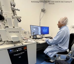
The goal at AlixLabs is to research more about the etching process on inclined surfaces of GaP wafer to make it more widely used and cost-efficient. By running simulations of its etching using different variations of plasma, including Chlorine, we were able to have approximate values of how much energy consumption is needed. Furthermore, by doing SEM analysis and Ellipsometry, we were also able to study the width of the wafers after each round of etching. The ALE process, devised by AlixLabs, has the potential to make nanostructures smaller than 20 nm – which will enable the placement of more transistors on one chip, allowing for an even faster response time for devices.
If successful in enabling this new method of ALE for large-scale use, this would be an economically affordable method and will also produce fewer by-products which are not sustainable. The faster response time and increased longevity of all the devices which use semiconductors, such as mobile phones and medical devices, will also contribute to reducing e-waste. The key challenge is increasing the consistency of the etch rate and improving the implementation of the Schrödinger software for our desired goal, and increasing the speed of the process.
Reflecting on our placement
 All in all, we really enjoyed the experience of being able to contribute our part and have this opportunity to travel to Sweden and learn more about AlixLabs and semiconductors. This has certainly deepened our knowledge in this research area, and we are very grateful to continue our alliance with them.
We plan on pursuing the modules of Optoelectronics and Nanomaterials in our years 3 and 4, which have semiconductors at the heart of their foundation. This placement has been a strong starting ground for us to apply the knowledge we have and will gain regarding fabrication and quantum mechanical effects of semiconductors directly into research.