 Dr Robert Hoye is a lecturer in the Department of Materials. In this post, he explains the potential for halide perovskites and their derivatives in renewable energy. Dr Hoye recently led one of the key roadmaps for the Henry Royce Institute, identifying halide perovskites as one of the key technologies for the UK to achieve carbon neutrality by 2050.
Photovoltaics produce clean electricity from sunlight and are one of the leading renewable technologies. As such, it is vital to accelerate the deployment of this technology. However, realising a high electrification future will require the number of photovoltaic devices installed every year to increase by over an order of magnitude. A rapid expansion in the manufacturing of photovoltaics is needed, and this may be fulfilled by a newcomer to the photovoltaics scene: halide perovskites.
What are halide perovskites?
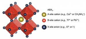
The term ‘perovskite’ refers to a family of materials with the crystal structure shown in Figure 1. The prototypical perovskite (calcium titanate) was found nearly 200 years ago in the Ural mountains by Gustav Rose, who named the material after Lev Perovskiy. Other perovskites include barium titanate, strontium titanate, lead titanate, and others, and these materials have been used in ferroelectrics, piezoelectrics and pyroelectrics. It was only recently that halide perovskites have come to prominence for photovoltaics.
In 2009, Tsutomu Miyasaka and colleagues reported methylammonium lead iodide as a sensitizer in liquid-junction solar cells, demonstrating a power conversion efficiency of 3.8%. In subsequent years, a series of developments transformed this material from yet another novel solar absorber to the dominant next-generation photovoltaic technology. In 2020, the certified record efficiency of perovskite solar cells reached 25.5%, which is already on the cusp of matching the record performance of solar cells based on single-crystalline silicon (26.7%), the dominant commercial technology. Remarkably, whilst crystalline silicon required 6 decades of development, halide perovskites have only been developed for one decade. Furthermore, halide perovskites hold several critical advantages over crystalline silicon:
1. Halide perovskites can be grown at significantly lower temperatures, with the absorber typically processed at only ~100 °C. This reduces the carbon footprint of perovskite solar cells, as well as the energy and cost required for its production;
2. Halide perovskites have significant chemical versatility, with the bandgap tunable over the entire visible wavelength range by controlling the composition or dimensionality.
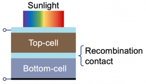
An important implication of these factors is that perovskite solar cells can be used to produce ‘tandem’ photovoltaics with silicon solar cells (Figure 2). Much like tandem bicycles, tandem photovoltaics electrically couple together two solar cells (in this case perovskites and silicon) to work together to generate more power. Such devices can exceed the efficiency limit of each device working individually. Critically, by adding a perovskite solar cell over a silicon solar cell, increases inefficiencies can be achieved without significantly adding to the total cost, thus reducing the ratio of the cost of the solar cell compared to the total power produced, such that photovoltaics become more cost-competitive against fossil fuels.
How perovskites photovoltaics be pushed from lab to market?
Halide perovskite solar cells have risen in efficiency faster than any other photovoltaic technology and are already at the level at which they can be commercialised. However, their fast rise has also meant that most research on this technology has been performed at the lab scale, in which the most efficient solar cells have device areas smaller than a fingernail. By contrast, manufacturing perovskite photovoltaics at the level needed to make an impact on climate change will require at least several million square metres of devices per year. Achieving this will require fabricating with speed and at scale. Perovskites can be grown over a large area by printing, spraying or evaporating, but it is critical that these techniques can grow devices rapidly in order to maximise the number of devices produced per manufacturing hour and therefore reduce the overall costs.
Another critical concern is the operating lifetime of the devices. The original perovskite composition, methylammonium lead iodide, is thermodynamically unstable and degrades in ambient air within days. There has been substantial work on developing alternative compositions, as well as passivating materials at surfaces, with improved stability in air containing moisture. Through these efforts, and coupled with encapsulation, devices stable for longer than a year have been demonstrated, and modules that pass industry-standard stability tests have been achieved. However, the stability tests were developed for silicon solar cells, and the degradation modes in perovskites can be substantially different. It will therefore be critical to developing accelerated degradation tests specifically for perovskites, and the field data that is starting to be collected will be valuable in this effort.
How can we systematically find lead-free alternatives to the perovskites?
Beyond the scale-up and stability challenges, halide perovskites are also limited by the presence of lead, which is toxic and regulated in many jurisdictions worldwide. Currently, outdoor photovoltaics are exempt from European lead regulations, and there is debate over the extent to which the lead content of halide perovskites could limit its adoption worldwide. Nevertheless, the astonishing rise of halide perovskites has posed the critical question of how such performance could be replicated in alternative materials.
The search for these lead-free alternatives has mostly proceeded in the same way solar absorbers were identified before lead-halide perovskites were found, that is by trial-and-error. Not only does this have a low success rate, there are also too many materials to systematically explore without encountering false negatives or positives.
A more systematic approach that has been adopted is to identify materials that could replicate the defect tolerance of halide perovskites. Developing defect-tolerant semiconductors is the opposite approach to traditional semiconductor engineering. Historically, the approach taken has been to grow semiconductors to minimise the density of defects, which usually involves high temperature, slow and expensive growth methods. What the lead-halide perovskites have shown is how materials can be efficient without being defect-free if most defects have energy levels close to the band-edges and have limited ability to capture electrons or holes. Thus, although halide perovskites have millions of times more defects than silicon, they have comparable performance in photovoltaic devices.
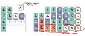
A proposition is that the defect tolerance of halide perovskites comes about from its electronic structure. This has prompted efforts to find materials that are electronically analogous. Many of the materials identified are bismuth-based compounds, such as bismuth oxyiodide. This is because bismuth is next to lead on the periodic table (Figure 3), but has no evidence for toxicity, and is used in over-the-counter stomach medicine. Such materials are termed ‘perovskite-inspired materials’. Thus far, there have been a handful of materials found to demonstrate similar defect tolerance to the halide perovskites. But the understanding of what gives rise to defect tolerance is only now emerging and is an active area of research.
What else can we use the new perovskites and derivatives for?
Demonstrating a new material in efficient photovoltaics opens up many possibilities for applying the material in a broad range of alternative applications. One such application is for indoor light harvesting. These energy-havesting devices are needed to power low-cost, low-power electronic devices that can communicate with each other via the Internet – such as a mobile phone. This ecosystem of devices is termed the ‘Internet of Things’ (IoT), which is giving rise to infrastructure (e.g., houses, cities, hospitals) that are responsive to the users. Currently, most IoT devices are powered by batteries, which only have a limited lifetime. Given that there are over tens of billions of IoT devices worldwide, millions of batteries need to be recycled daily, creating substantial waste. This sustainability challenge will only increase in the future as the IoT ecosystem exponentially grows in size.
To solve this challenge, photovoltaics can be embedded into each IoT device to harvest energy from light to recharge the energy storage device (which could be a capacitor or a rechargeable battery) that then powers the IoT device in the dark. Currently, the standard indoor photovoltaic material is hydrogenated amorphous silicon, but the photovoltaic efficiencies are below 10% under indoor lighting. Halide perovskites have already demonstrated 37% efficiency indoors, which increases the power harvested from the microwatt range to the milliwatt range.
However, lead may be less tolerated in consumer or healthcare products than for outdoor photovoltaics. Recent work into lead-free perovskite-inspired materials for indoor photovoltaics, and optical analyses has shown that devices made from these materials could match or exceed the performance of halide perovskites indoors, and deliver high efficiencies with non-toxic materials that can be manufactured through low-toxicity processes. Beyond indoor light-harvesting, halide perovskites and perovskite-inspired materials can be used to harvest sunlight to split water and CO2 to produce clean fuels, or to more effectively detect X-rays, and therefore be used to make safer medical detectors.
Further reading
C. A. R. Perini, T. A. S. Doherty, S. D. Stranks,* J.-P. C.-B.,* R. L. Z. Hoye.* Pressing Challenges in Halide Perovskite Photovoltaics – From the Atomic to Module Level. Joule, 2021, 5, In Press. DOI: 10.1016/j.joule.2021.03.011
R. L. Z. Hoye,* J. Hidalgo, R. A. Jagt, J.-P. Correa-Baena, T. Fix,* J. L. MacManus-Driscoll.* The Role of Dimensionality on the Optoelectronic Properties of Oxide and Halide Perovskites, and their Halide Derivatives. Advanced Energy Materials, 2021, 2100499, Early View. DOI: 10.1002/aenm.202100499.