MSc spotlight: Srikar Varanasi on his MSc journey and research project
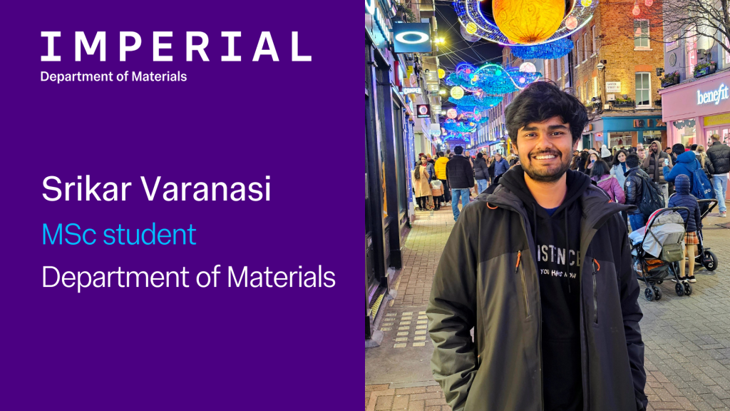
Name: Srikar Varanasi
Position: MSc student studying Advanced Materials Science and Engineering.
In this blog post, Srikar shares more about his journey in the Department of Materials at Imperial College London.
Why did you choose to study for an MSc in Advanced Materials Science and Engineering?
With a background in mechanical engineering, I spent years learning about mechanics, dynamics, and the intricacies of designing and analyzing mechanical systems. However, I was curious about what makes materials behave the way they do. What gives materials their strength? How are they made? What happens at the atomic level when materials interact? And how do you study them? This curiosity led me to materials science, a field that sits at the intersection of chemistry, physics, and engineering, providing answers to these questions and offering endless possibilities for innovation. When it came to choosing where to further my studies, Imperial stood out with its strong reputation in research and the opportunity to work with some of the brightest minds in the field, making it the perfect choice.
What do you enjoy about studying at Imperial?
Living in London has been a childhood dream come true. The city is a melting pot of cultures, offering endless opportunities for  exploration and entertainment. Whether it’s visiting world-renowned museums, exploring myriad parks and historic landmarks, or indulging in the vibrant food scene, there’s always something to do.
Moreover, being in London means being at the heart of a major global city which is a hub for many industries and, of course, research. The proximity has provided me with opportunities for networking and attending industry conferences and events. Another great aspect of studying at Imperial is its student diversity. I have met people from various parts of the world, each bringing their unique perspectives and experiences. This diversity enriches classroom discussions and group projects, making the learning experience more holistic.
What have you enjoyed about the course?
The course has been both challenging and rewarding. I have chosen to study the ceramics modules and materials characterization exercise was a great learning experience. Having no prior experience in characterization techniques, the exercise helped me grasp how materials are studied at a fundamental level.
As a student from a different background, the course has given me enough time to catch up with my peers. Even though it is just one year long, it doesn’t feel rushed. The pacing has been well-balanced, allowing for deep dives into complex topics without feeling overwhelming. The course includes seminars and guest lectures from industry leaders and researchers, providing insights into the latest advancements and trends in materials science. These opportunities to learn from and network with professionals are invaluable.
Can you tell us about your summer project?
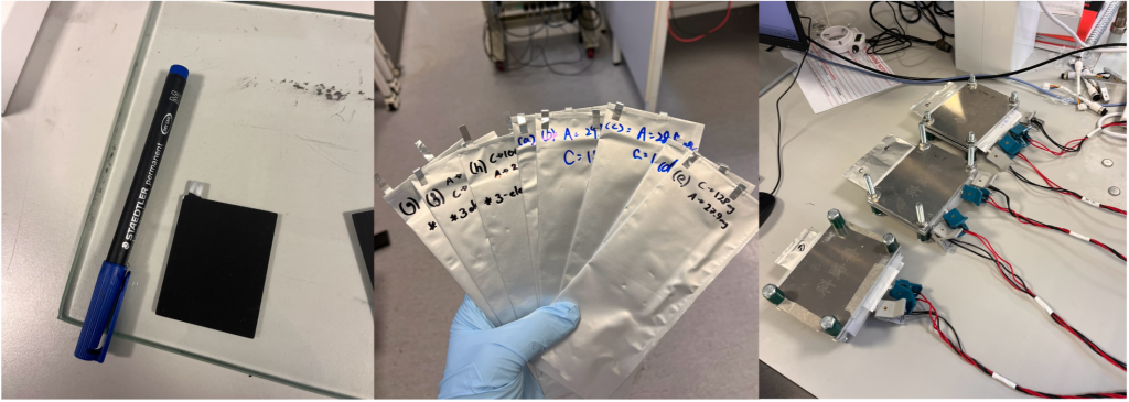
This summer, I’m working on an exciting project related to composite materials, specifically focusing on Carbon Fibre Reinforced Polymers (CFRP) used in offshore pipelines. The aim of my research is to understand how these composite materials degrade when exposed to petroleum products, ultimately leading to failure.
CFRP is widely used in the oil and gas industry due to its high strength-to-weight ratio and excellent corrosion resistance. However, the harsh environmental conditions in offshore applications, combined with prolonged exposure to petroleum products, can lead to degradation over time.
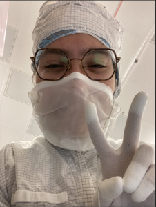
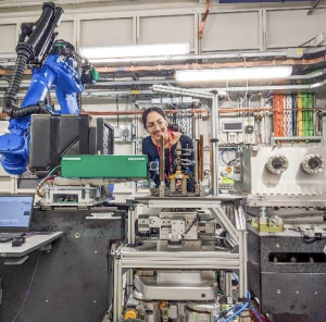
My project involves simulating these conditions in the lab to study the degradation mechanisms at play. Through a series of experiments, I’m analysing how components of petroleum interact with the interface between the polymer matrix and carbon fibres, which is the most crucial part responsible for transferring the stress from the matrix to the fibres, thus giving them strength in the first place. This involves using advanced material characterization techniques such as in-situ SEM techniques to observe changes in the microstructure and mechanical properties of the composites.
Why did you study this area and why is it important?
This research is crucial because it addresses a significant challenge in maintaining the integrity and safety of offshore pipelines. By improving our understanding of material degradation, we can help prevent pipeline failures, which can have severe environmental and economic consequences.
Prior to this, I worked on the structural integrity of aircraft structures using CFRP during my undergraduate project. This experience gave me a solid foundation in understanding the mechanical properties and advantages of CFRP in high-stress applications. It also sparked my interest in exploring how these materials perform in different environments, leading me to my current research on their degradation in offshore settings.
What’s something others would be surprised to learn about you?
I’m an avid explorer and hiker. I have a deep love for adventure and discovering new places. I’m known for embarking on journeys where I’d happily walk 40,000 steps if it meant encountering something I’d never seen before. Whether it’s trekking through rugged mountains or exploring hidden trails, I find joy in immersing myself in nature and embracing the thrill of exploration.
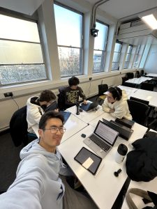 One of the top reasons I enjoy studying Material Science and Engineering at Imperial is the mix of coursework and exams within the degree program. I’m currently going strong in my second year (I hope!) and I have already completed over ten labs, where I’ve conducted interesting experiments like polymer synthesis and cooling curve measurement.
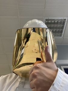 It is always exciting when what you learn connects with the real world. During my summer internship at SKF Sweden, I saw and applied many skills from my first year. The sample preparation skills I learned came in handy when I cut, ground, and polished various bearing samples. My understanding of steel phase diagrams also allowed me to hold insightful conversations with the company’s heat treatment expert. Now in my second year, many things that I didn’t understand before are becoming clearer and clearer.
 I first became interested in Materials Science and Engineering because I wanted to understand what makes certain things more fragile than others or more susceptible to breaking and failure! This is only the smallest part of Materials Science and Engineering, as I would discover during my time at Imperial.
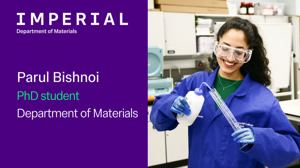
 I’m part of two research groups. My main supervisor is Dr Stella Pedrazzini and my secondary supervisor is Professor Mary Ryan. My project is supervised by two successful women and I’m fortunate to work in a diverse and inclusive environment. Recently, some of our research group members, including myself, attended the TMS Conference in Florida.
 I like to unwind from my PhD by trying out new recipes, whether cooking or baking. As science experiments tend to require careful measurements, cooking is generally more flexible and gives me the chance to be slightly more creative. I also enjoy practising creativity through art, especially hyper-realistic drawings and paintings.