Inside the workshop: With Russell Stracey and Mike Lennon
The RSM workshop, located on the lower ground floor of the Royal School of Mines, serves as a central machining facility providing design and manufacturing support for all three Departments within RSM: Materials, Bioengineering and ESE. It has a comprehensive range of both manual and CNC machines; some of the manual machines date back to the old Metallurgy workshop and have been in operation since the 1960s.
Russell Stracey, RSM Workshop Manager, became a part of the workshop team in 2008, while Mike Lennon, Mechanical Workshop Technician, joined in 2013. We had the opportunity to speak with Russell and Mike to learn more about the workshop’s evolution over time, exciting projects, and their personal highlights.
Can you tell us more about the workshop?
 Mike: Workshops are important to produce of a wide range of goods. When you think about it, everything around you is likely created in a type of workshop, from transport to household items and clothing – it just depends on the size, scale, and capability of the facility. In the Department of Materials, we focus on making components that can support research or teaching – and we are always up for a new challenge!
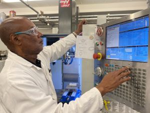
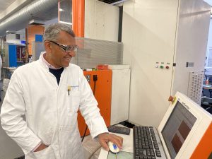
Russell: When you look around our workshop, there are a range of drilling, cutting and creating machines – both old and new. The workshop’s physical layout has undergone significant transformations throughout the years. When I arrived in 2008, it was three times its current size and occupied multiple floors! Furthermore, our team has expanded, welcoming additional staff members. Over time we have introduced CNC machines alongside traditional manual machines, enhancing our operational efficiency. Some of the old machinery still has a valuable purpose in supporting our work – the oldest facility here dates to the 1960s!
What’s a typical day like?
Russell: A typical day for us can be quite varied! We usually focus on machining experimental components for our PhD students and researchers to support their projects across a wide range of disciplines, from engineering alloys to medical and energy applications. We also manufacture samples for tensile testing that our UG students use during their labs
 Most parts machined in the workshop are made from metal or plastic. In recent years, we have witnessed a growing demand for the use of new materials such as Peek. Peek is a fairly new material. It has become an increasingly popular material, replacing PTFE for sample holders, as it doesn’t contaminate the material which is being tested, is a more stable material from a machining perspective and is able to operate at higher temperatures.
Can you tell us more about collaborations and projects that you have been involved with?
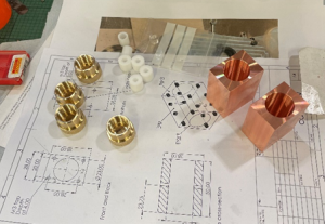
Mike: We have opportunities to be involved with unique research projects. For example, I enjoyed machining parts to support Professor Neil Alford with his research into diamond masers (a microwave laser) which work at room temperature. This idea was suggested in the 1970’s but no one had managed to create a diamond maser because they all used microwave cavities – a metallic cylinder with connectors – made by the manufacturer of the big magnets used in the experiment. Professor Alford asked if I could create a cavity in oxygen free copper to support the world’s first diamond maser. The group are now trying to miniaturise the device, so I’m helping to build microwave cavities for this research.
Russell: We’ve also machined parts to support the ‘design study’ projects created by our undergraduate students. Sometimes, they just needs a small part or tweak to get it working properly! Recently we have created hundreds of custom ‘materials bucky ball’ key rings for the Great Exhibition Road Festivals and Open Days too, which was a new challenge!
 What do the team most enjoy about their roles in the workshop?
Russell: What I enjoy most about the role is meeting people and working with the team. In the workshop, you get to work with many people with great ideas for making the world a better place. If we can be just a small part of that stepping stone to support their research, it can feel very rewarding.
Mike: I’ve really enjoyed the opportunity to train our apprentices. I first started training apprentices 11 years ago, and I’m currently training my last! It’s been fantastic to see younger technicians learn new skills over the years and take these forward in their new roles.
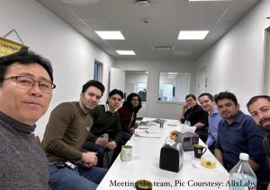
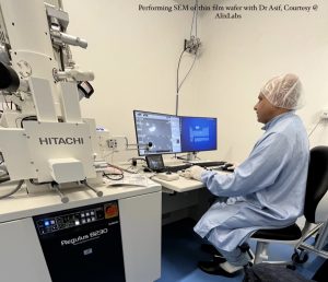 The newly discovered method at AlixLabs allows ALE to be selectively performed on inclined surfaces – which in turn can be fabricated by epitaxial growth and dry etching. Our task was to get an approximate of how GaP (Gallium Phosphide) will be etched if chlorine (Cl) was used as the plasma and obtain the values of surface energy required for it. To achieve this, we used the Espresso and Jaguar software provided through Schrödinger, which allowed us to build a GaP crystal and turn it into a slab having some amount of vacuum space. Upon adding a Cl
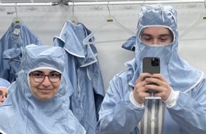 All in all, we really enjoyed the experience of being able to contribute our part and have this opportunity to travel to Sweden and learn more about AlixLabs and semiconductors. This has certainly deepened our knowledge in this research area, and we are very grateful to continue our alliance with them.
 I work on the environmental degradation of engineering alloys. I look into the oxidation and hot corrosion of nickel and cobalt based superalloys and aqueous corrosion of steel. To this day, very few research groups around the world work on corrosion due to the challenges involved in this type of investigation. My research group also consists of mostly women – which is very unique in STEM. I also teach the 1st year undergraduate module in Materials Electrochemistry.
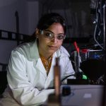
 Light contains so much information about all the materials in nature. The more in-depth we analyse all the shades of light interacting with matter, the richer details are revealed and nanotechnology helps boost light-matter interactions. I utilise nanotechnology to develop smart sensing platforms boosting these light-matter interactions to detect disease biomarkers. We expect that the sensing platform would allow for fast screening of diseases, and therefore the early detection and treatment of diseases in the future.
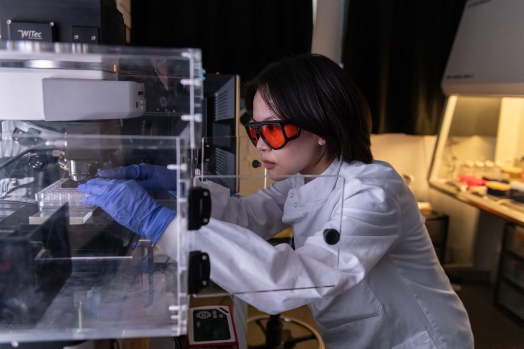
 I am the facility manager for the
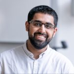
 I work on discovering active, stable and low-cost materials that can catalyse green hydrogen production from water using renewable electricity.

 In this post, Nomaan Nabi, Research Postgraduate in the Department of Materials, explains more about Ramadan and how he balances fasting with his research during the holy month.
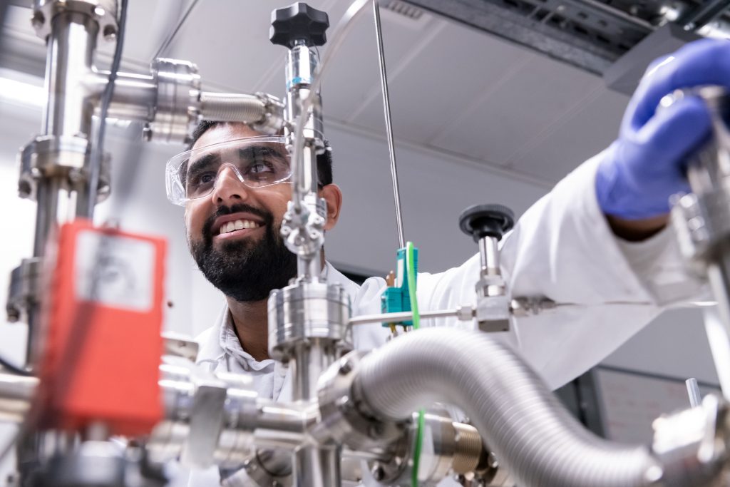
 Dr Anna Klöckner is a Marie Skłodowska-Curie Fellow in the Department of Materials. Her research focuses on finding novel treatment strategies to overcome the problem of antibacterial resistance. She works within the Stevens Group and the Edwards Group (Microbiology, CMBI).
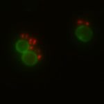
 Dr Sam Humphry-Baker is an Imperial College Research Fellow in the Department of Materials. His research lies at the intersection of materials science and fusion engineering, where he develops new materials that can enable fusion energy reactors to be deployed on a smaller scale.